DIGITAL PRODUCT MARKETPLACE
Latest Digital Experiences and The Power of AI
- Art
- Band Performance
- Business
- Causes
- Childrens
- Comedy
- Concert
- Crafts
- Dance
- Drinks
- Education
- Exhibition
- Farmer's Market
- Film
- Fitness
- Food
- Fundraising Auction
- Fundraising Dinner Party
- Games
- Garage Sale
- Gardening
- Gay Parade
- Hackathon
- Health
- Home
- Literature
- Local Sport Competition
- Masquerade
- Music
- Networking
- Open House
- Party
- Religion
- Shopping
- Speed Dating
- Sports
- Theatre
- Wellness
- Wine Tasting
- Custom Event
- Airfield
- Amusement Park
- Bench
- Campsite
- Cemetery
- Circle
- Circle Stroked
- Clock
- Common
- Dog Park
- Drinking Water
- Entrance
- Event Location
- Ferry
- Ferry Terminal
- Firepit
- Fountain
- Harbor
- Heliport
- Marker
- Monument
- Mountain
- Nameplate
- Nature Reserve
- Park
- Parking Entrance
- Parking Space
- Picnic Site
- Picnic Table
- Playground
- POI
- Prison
- Rail
- Rail Light
- Rail Metro
- Rocket
- Slipway
- Star
- Town Hall
- Triangle
- Triangle Stroked
- Volcano
- Water Point
- Custom PoI
- Adult Gaming Centre
- Agrarian
- Airport
- Alcohol Shop
- Amusement Arcade
- Animal Boarding
- Animal Shelter
- Appliance
- Aquarium
- Art Gallery
- Attraction
- Automotive
- Baby Goods
- Bakery
- Bank
- Bathroom Furnishing
- Beach Resort
- Beauty
- Beer
- Bicycle
- Bicycle Parking
- Bicycle Rental
- Bicycle Repair Station
- Bicycle Share
- Bird Hide
- Boat Rental
- Bookmaker
- Bowling Alley
- Brothel
- Bus
- Business
- Butcher
- Cafe
- Car
- Car Rental
- Car Sharing
- Casino
- Castle
- Cheese
- Childcare
- Cinema
- Clothing Store
- Club
- College
- Coworking Space
- Craft
- Curtain
- Dairy
- Dance
- Dentist
- Department Store
- Dive Centre
- Doctor
- Dojo
- Driving School
- E-Cigarette
- Electrical
- Embassy
- Escape Game
- Estate Agent
- Events Venue
- Farm
- Fashion
- Fast Food
- Finance
- Fire Station
- Fishing
- Fishmonger
- Fitness Centre
- Fitness Station
- Food
- Frame
- Fuel
- Funeral Directors
- Gambling
- Games
- Garden
- Gas
- Glaziery
- Golf
- Grocery
- Gym
- Hackerspace
- Health Food
- Herbalist
- Hobby
- Horse Riding
- Hospital
- Hotel
- Household
- Houseware
- Hunting
- Hunting Stand
- Ice Cream
- Ice Rink
- Information
- Insurance
- Internet Cafe
- Kitchen
- Labor Move
- Language School
- Laundry
- Law Office
- Leather
- Lessons Tutoring
- Library
- Lighting
- Locksmith
- Lodging
- Lottery
- Love Hotel
- Medical
- Medical Supply
- Monastery
- Money Lender
- Money Transfer
- Motorcycle Parking
- Motorcycle Repair
- Museum
- Music
- Nutrition Supplements
- Office
- Organic
- Paint
- Parking
- Party
- Pastry
- Pawnbroker
- Payment Centre
- Payment Terminal
- Pet Grooming
- Pharmacy
- Photo Studio
- Pitch
- Place Of Worship
- Police
- Post
- Prep School
- Printing
- Private Toilet
- Public Bath
- Public Bookcase
- Radiotechnics
- Ranger Station
- Recycling
- Register Office
- Religion
- Religious Christian
- Religious Jewish
- Religious Muslim
- Rentals
- Resort
- Restaurant
- Retail Store
- Sauna
- School
- Scuba Diving
- Seafood
- Sewing
- Shelter
- Shoe Repair
- Shop
- Shower
- Software
- Spa
- Sports Centre
- Stables
- Stadium
- Storage Rental
- Stripclub
- Studio
- Suitcase
- Swimming
- Swimming Pool
- Tanning Salon
- Tea
- Telephone
- Theatre
- Theme Park
- Tiles
- Toilet
- Toilets
- Track
- Trade
- Training
- Tyres
- Vacant
- Vacuum Cleaner
- Vehicle Inspection
- Vending Machine
- Veterinary
- Waste Basket
- Waste Disposal
- Water
- Water Park
- Wilderness Hut
- Window Blind
- Wine
- Yes
- Zoo
- Custom Business
Real Estate
Tools
Commercial
Vehicles
Real Estate
-
Apartment

-
Room

-
Garage

-
Villa

-
House

Tools
-
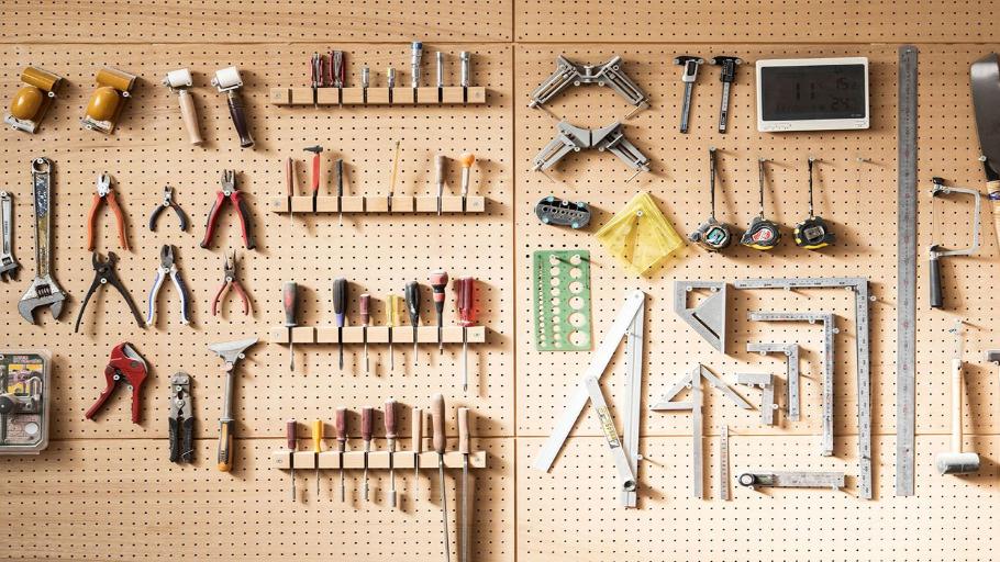
Tools
Commercial
-
Office

-
Commercial Space

-
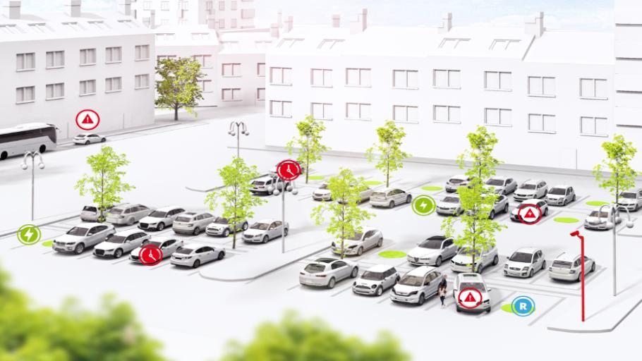
Parking
-
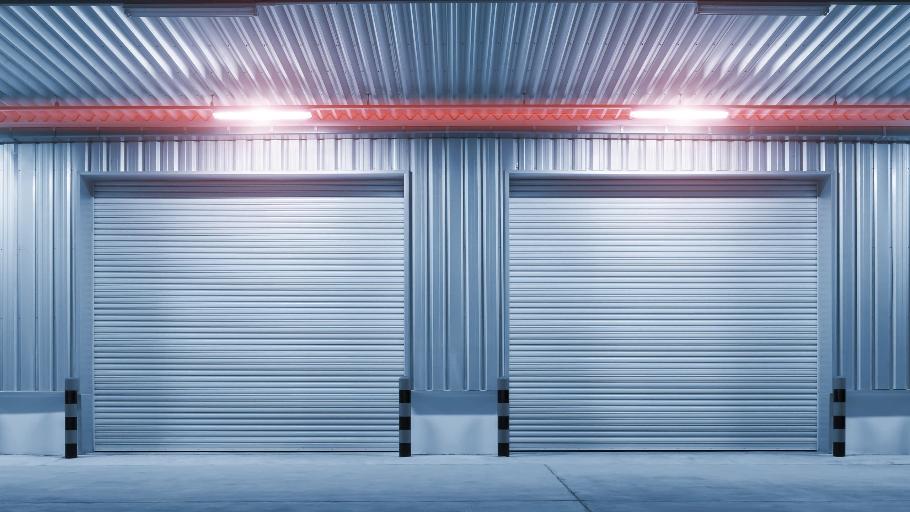
Storage
Vehicles
-
Boat

-
Car

Family
Art
Sports
Online
Outdoor Activities
Lessons
Consulting
Services
Unwind
Relax & Beauty
BnB
Family
-
Kids Quest

-
Inflatables

-
Farm Visit

-
Fine Dining

-
Pet Care

-
Horse Back Ride

- Baby Sitting
- Face Painting
- Personal / Family Assistant
Art
-
Tattoo Artist

-
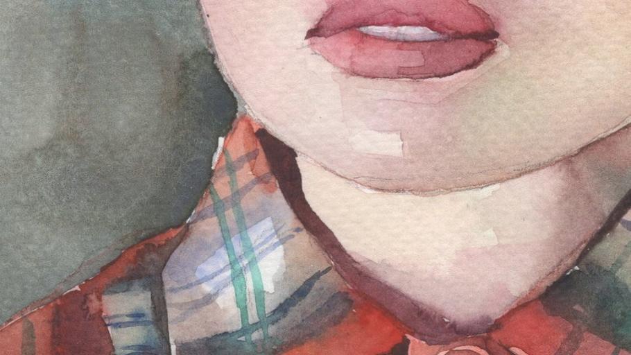
Watercolor Portrait
Sports
-
Self Defense Lessons

-
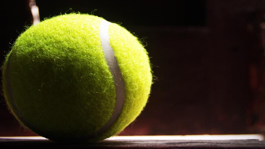
Field Tennis
-
Group Meditation

-
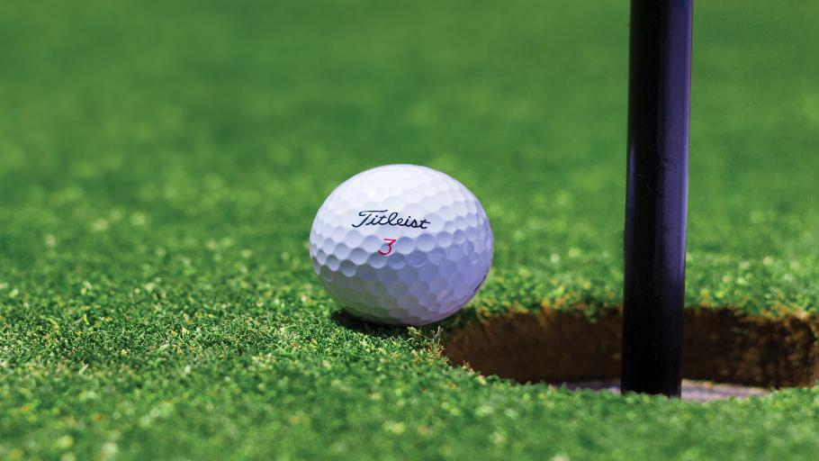
Golfing
-
Running Training

-
Fitness Training

- Wellness Lesson
- Cycling Tour
- Yoga Session
Online
-
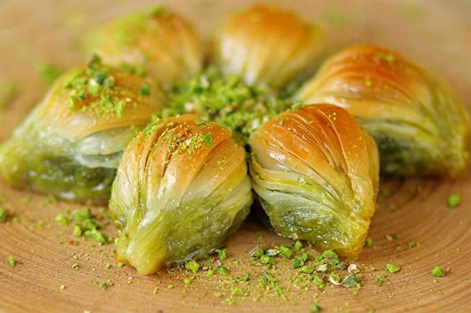
Turkish Baklava
-
Cooking Lesson

-
English Lesson

-
Online Virtual Date

-
Piano Lesson

Outdoor Activities
-
Experience

-
Fishing Lesson

-
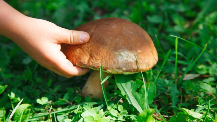
Mushroom Picking
-
Forest Camping

-
Show Me Around

-
Gardening
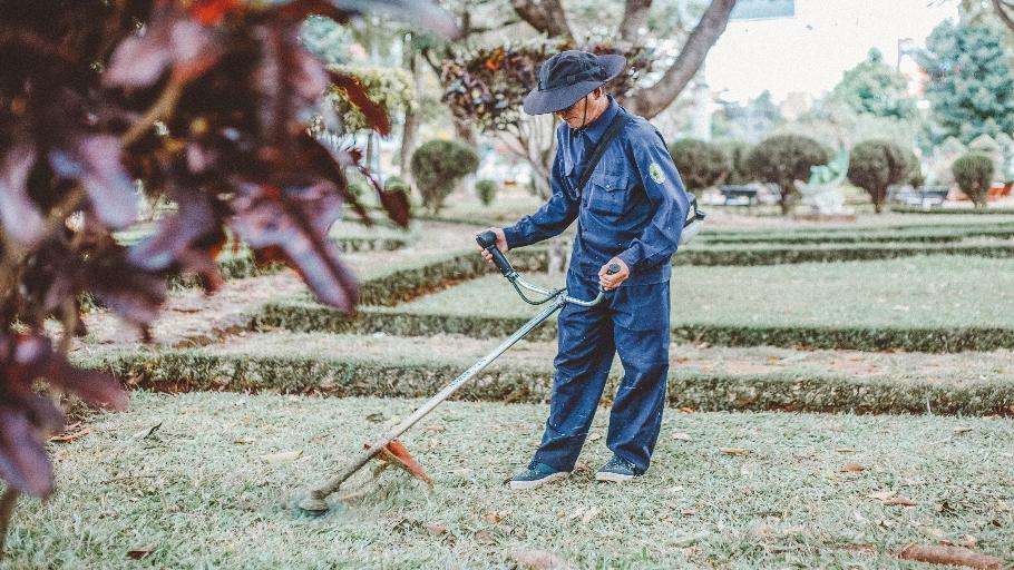
- Roller Skating Ride
- Sailing Adventure
- Kayak Wild Camp
- Hiking Adventure
- Hunting
Lessons
-
Math lessons

-
Voice Lessons

-
Guitar Lessons

-
Violin Lessons

Consulting
-
Second Opinion
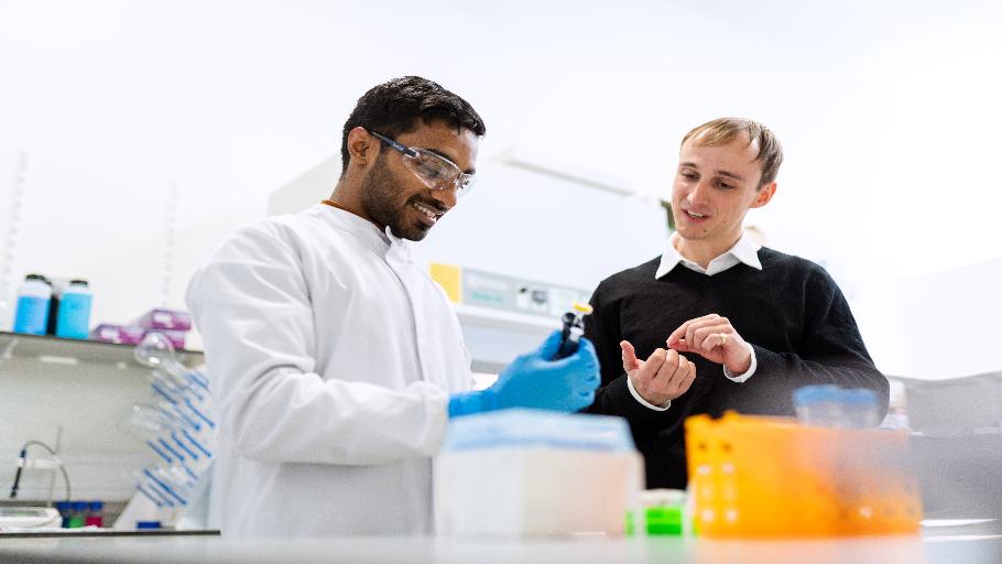
-
Business Lunch

-
Private Investigation

-
Attorney Consultation

Services
-
Gardening Service
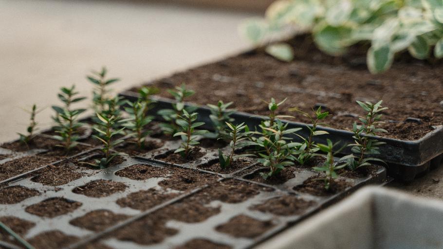
-
Dentist Visit

-
Delivery Service

-
Catering Service

-
Remodeling Service

-
Heavy Lifting Help

- Handyman Help
- Cleaning Service
Unwind
-
Walking Buddy

-
Girls’ Night Out

-
Adventure Buddy

-
Jump in My Car

-
Party

-
Beer Tour

- Wine Tasting
- Friend for a day
- Grab a Coffee Speed Date
Relax & Beauty
-
Fashion Nails

-
Massage Therapy

-
Hair Styling

-
Aroma Therapy

BnB
-
Bed & Breakfast

-
Stay On The Boat

-
Apartment

- Application
- Delivery Service
- Online Shop
- Website
- Custom Virtual Store
Repair and technical
Writing and translation
Repair and technical
-
Computer Repair
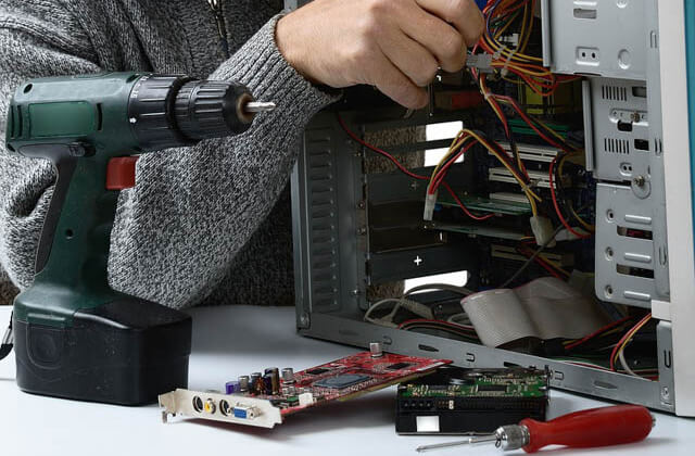
-
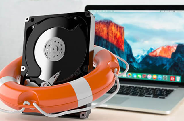
Data Recovery Service
-
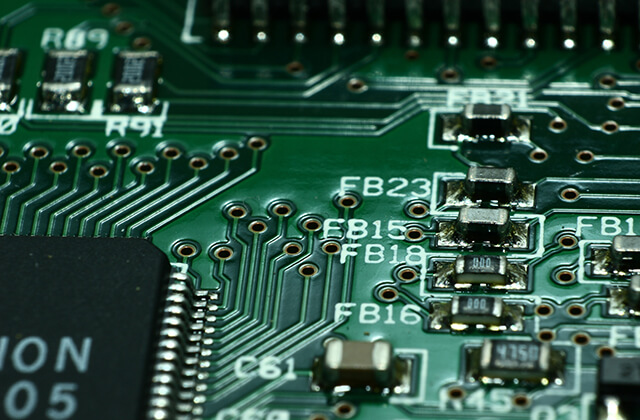
Electronics
-
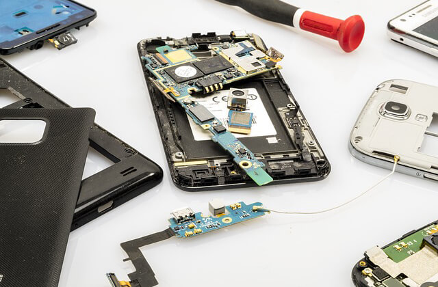
Mobile Phone Repairs
-
Network Support Services

-
Printer and Copier Repair

- Tablet Repair
Writing and translation
-
Write/Translate

-
none

-
custom

- S.O.S.
- Emergency
- Urgent Care
- Medical Assistance
- Carpentry
- Cleaning
- Construction
- Decoration
- Deep Clean
- Delivery
- Electrician
- Errands
- Event Staffing
- Executive Assistant
- Furniture Assembly
- Guy With a Truck
- IKEA Assembly
- Laundry and Ironing
- Lift & Shift Furniture
- Minor Home Repairs
- Mounting
- Moving Help
- Office Administration
- Organization
- Packing & Unpacking
- Painting
- Pet Sitting
- Petition
- Plumbing
- Sewing
- Shopping
- Transportation
- Waiting in Line
- Window Cleaning
- Yard Work & Removal
- Custom
- Accident
- Injury
- Contagious Area
- Crime
- Abuse
- Assault
- Vandalism
- Outbreak
- Natural disaster
- Dangerous zone
- Custom
